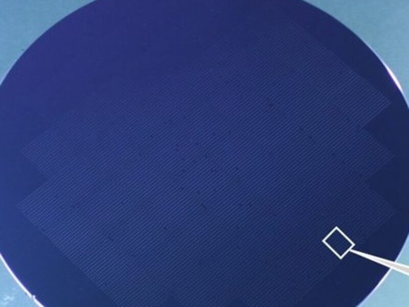
Tiling process mounts InP optical devices on 300mm substrate
 Cette publication existe aussi en Français
Oki Electric Industry in Japan has used its crystal film bonding (CFB) technology to mount optical components from 50mm wafers on larger 300mm silicon wafers.
The Tiling CFB approach allows the heterogeneous integration of small-diameter optical semiconductor wafers on mainstream 300 mm silicon wafers for high volume production of chips with high speed photonic interfaces. This was not previously possible on large wafers, says Oki, which is working with partners and the Nishiyama Laboratory at Institute of Science in Tokyo on the commercialization.
AI in particular is driving the demand for high speed chip to chip links with lo power consumption, a key target for photonics. Optical semiconductor wafers such as InP (indium phosphide) wafers are typically smaller 50 mm (2in) to 100 mm (4in) compound semiconductor wafers due to the difficulty of achieving epitaxial growth. Additionally, silicon optical waveguides require nanoscale roughness control, which in turn requires heterogeneous integration processes that avoid causing damage.
- Cornerstone aims for a Github of photonics
- World’s first photonic processor fires up
- Nvidia looks to silicon photonics to cut AI datacentre power consumption
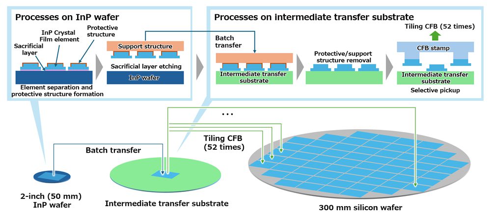
The CFB technology was originally developed by OKI for its printers, and the tiling approach overcomes the disparity in wafer sizes with 52 repeated tiling operations over the entire surface of a 300 mm silicon wafer using a single 50mm InP wafer, enabling efficient use of InP-based materials in just 10 minutes.
The InP wafer can be reused as is after transfer to allow material recycling and reuse, helping reduce the environmental burden. Placement accuracy is approximately ±1 μm, with an angular accuracy of ±0.005°. This high accuracy, when combined with OKI’s proprietary 3D intersecting waveguide silicon photonics technology, allows high-efficiency optical coupling between optical semiconductors and silicon waveguides even with a misalignment of approximately ±3 μm.
Source: Oki
In a demonstration, a sacrificial layer and InP-based Crystal Films functioning as optical semiconductors were epitaxially grown on a 50mm InP wafer, then separated into individual elements.
A protective structure to prevent chemical attack when etching the sacrificial layer and a support structure for batch transfer were formed on each element. This enabled the InP-based Crystal Films to be successfully batch-transferred to an intermediate transfer substrate without erosion.
Batch transfer to an intermediate transfer substrate is carried out to protect the silicon wafer from damage during the subsequent removal process, as removing the protective structure and support structure on the intermediate transfer substrate prevents damage to the silicon wafer during the removal process.
The design of the intermediate transfer substrate ensures that the InP-based Crystal Films do not peel off, maintain adhesion during the process of removing the protective structure and support structure, and are easily transferred during the transfer process.
The 30 x 30mm CFB stamp has a structure capable of selectively transferring only the Crystal Films required, and repeated transfer enables efficient tiling. The capacity to repeatedly transfer lower-density arrays of Crystal Films required for the device from a high-density array of Crystal Films arranged on the intermediate transfer substrate allows effective use of materials without waste.
The technology can also be adapted as necessary to allow use with 75mm and 100mm InP wafers and 200mm silicon wafers. It can also be applied with existing optical semiconductor products for high heat-dissipation substrates and productivity by allowing use of larger wafer sizes.
 If you enjoyed this article, you will like the following ones: don't miss them by subscribing to :