Sensing boost for Europe at ISSCC
Sensing is a key technology in Europe to take advantage of the analog and mixed-signal expertise skills and manufacturing infrastructure.
The latest developments from European researchers highlight a single chip spectrometer that is a key step to integrating more measurement capabilities into electronic equipment as well as a chip with 1280 channels for the next generation of brain interface.
A paper at the recent International Solid State Circuit Conference (ISSCC2026) highlighted work by Xiaolin Yang at imec and KU Leuven in Belgium on a high-density neural probe for advanced neuroscientific research that is built on a standard 130nm silicon on insulator (SOI) process technology. The interface chip has 1280 electrodes for dense recording, 88 emission sites using thermos-optic switching and on-chip calibration to improve stimulation precision. This enables a probe for simultaneous opto-stimulation and recording in complex neural circuits, such as the hippocampus, to study brain behaviour and function.
The 1280 electrodes allow for extensive mapping of neural activity while the dual wavelength allows for targeted stimulation of brain sites with different colours to provide bidirectional, simultaneous neural manipulation.
Nanopores for molecular sensing
Other researchers from imec have also shown the first successful wafer-scale fabrication of solid-state nanopores using extreme ultraviolet (EUV) lithography. Solid-state nanopores are emerging as powerful tools for molecular sensing but haven’t been commercialized yet. This proof of concept is a crucial step towards their cost-effective (mass) production.
Nanopores are tiny holes just a few nanometres wide that are etched into silicon nitride membranes. When immersed in fluid and connected to electrodes, they allow individual molecules to pass through, generating electrical signals that can be analysed in real time. Because the pore size can be easily adjusted, the nanopore array offers a wide range of applications, from virus identification to DNA and protein analysis. This label-free, single-molecule detection method is key to next-generation diagnostic systems and even molecular data storage applications.
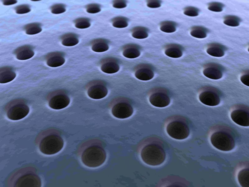
Nanopores developed at imec Image: imec
The imec researchers built highly uniform nanopores with diameters down to ~10nm across full 300mm wafers. The process combines EUV lithography with a spacer-based etch technique to achieve nanometre-level precision and reproducibility – two long-standing challenges in nanopore technology.
The nanopores were embedded in silicon nitride membranes and electrically characterized in aqueous environments. Translocation experiments with DNA fragments also confirmed high signal-to-noise ratios and excellent wetting behaviour, which confirms the sensor performance with biological material.
“Imec is uniquely positioned to make this leap. We can apply EUV lithography – traditionally reserved for memory and logic – to life sciences. By leveraging our lithography infrastructure, we’ve shown that solid-state nanopores can be fabricated at scale with the precision needed for molecular sensing,” said Ashesh Ray Chaudhuri, R&D project manager at imec. “This opens the door to high-throughput biosensor arrays for healthcare and beyond.”
Building upon the EUV nanopore advancements, imec is currently developing a modular readout system with scalable fluidics as a platform for application-relevant chemistry development. At ISSCC it showed a 256-channel event-driven readout chip that provides a 1MHz bandwidth and low noise down to 193pA for next generation solid state nanopore sensor arrays.
On chip spectrometer
Researchers at CEA-Leti and the Molecular Systems and (Nano)Materials for Energy and Health Laboratory (SyMMES) in France have developed a chip-scale electron paramagnetic resonance (EPR) spectrometer that achieves unprecedented scan speed, spectral span, and sensitivity from a battery-operated integrated circuit.
By replacing the bulky electromagnets used in conventional EPR instruments with an ultra-fast frequency-scanned architecture, the system enables high-performance paramagnetic sensing in portable and space-constrained environments where traditional systems cannot operate.
SyMMES is a key research unit that brings together staff from CEA, the French National Centre for Scientific Research (CNRS), Grenoble-Alpes University, and Grenoble INP Graduate schools of Engineering and Management, Université Grenoble Alpes.
The 14 GHz EPR-on-a-Chip is uses an injection-locked phase detection architecture that allows scanning at 1400 THz/s for a miniaturized EPR spectrometer with a 200 ns scan time across the full span. The 96mW power consumption allows portable, low-power chips capable of detecting reactive chemicals in energy storage, materials reliability, environmental safety, and biomedical processes. By eliminating the bulky electromagnet that traditionally limits EPR instruments to centralized facilities, the technology allows high-precision analysis directly in the field, at industrial sites, or inside research systems where traditional tools don’t fit.
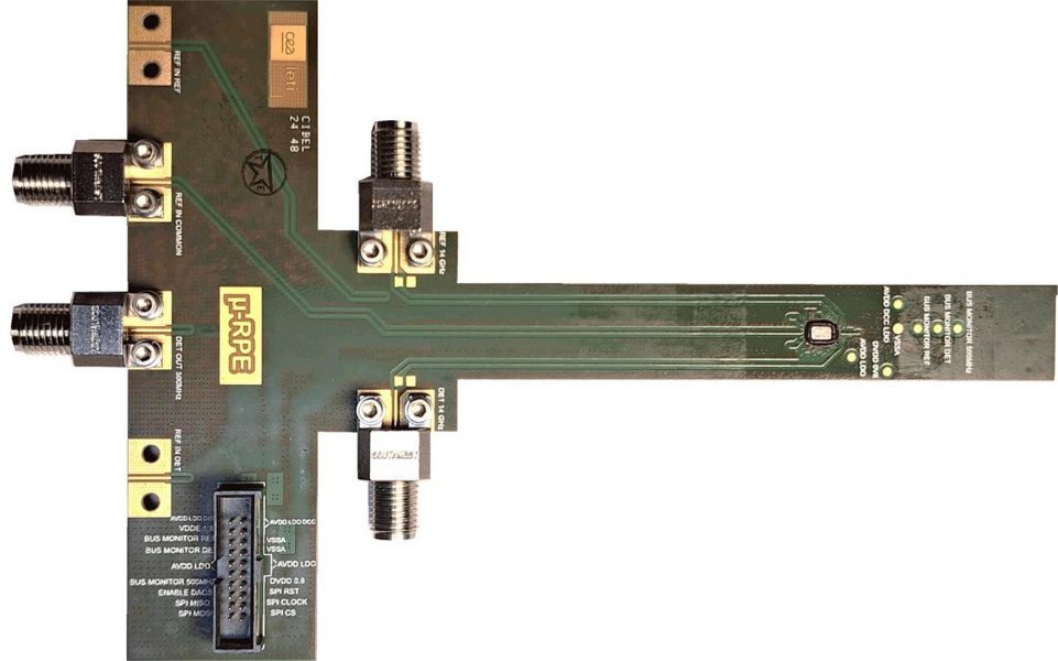
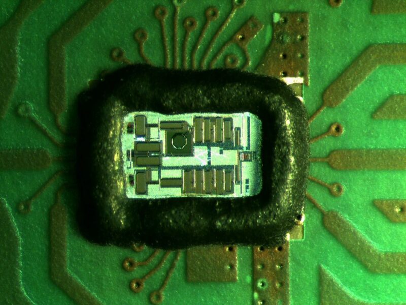
The spectrometer on a board Image: CEA-Leti
The injection-locked phase-detection architecture that encodes the EPR signal as a phase shift rather than an amplitude or frequency change. By exploiting the intrinsically low phase noise of injection-locked oscillators, the design achieves unprecedented sensitivity for a single-sensor, chip-scale EPR system.
“Our goal is to create a compact, portable EPR spectrometer that operates on just a few watts of power, enabling on-site analysis in environments where conventional instruments simply cannot operate,” said Serge Gambarelli, research director at CEA-IRIG and EPR spectroscopy expert.
“By adapting RF and frequency-synthesis architectures originally developed for telecommunications, we were able to integrate a complete EPR system on a single 22 nm chip,” said Alexandre Siligaris, senior research engineer at CEA-Leti.
The chip is built on 22 nm FDSOI technology at GlobalFoundries in Dresden, Germany. The system architecture, circuit design, and measurement approach were fully developed and patented by CEA.
“Typically applied in electric mobility and energy transition sectors, this expertise is now being leveraged to design the magnetic system for the µ-EPR spectrometer, demonstrating a valuable transfer of knowledge into the field of instrumentation,” said Celine Delafosse, laboratory manager at CEA-Liten, which is leading that research area.
This performance exceeds that of state-of-the-art miniaturized EPR devices, which typically trade sensitivity and spectral range for speed. The combination of ultra-fast scans and wide spectral coverage enables observation of fast-passage effects and transient phenomena in chemical reactions that are difficult or impossible to capture with existing systems.
The next step is to develop a full prototype for sensing, the technology represents a significant step toward making high-precision spectrometry more accessible and deployable beyond the laboratory.
There was more research at ISSCC 2026 from Dutch university in TU Delft on precision analog interfaces, medical imaging and ultra-low-power environmental sensing. Working with imec, the team showed an ultrasound-powering transmitter designed for brain implants. It uses a technique called Standing-Wave Peak Tracking and adiabatic power sensing to achieve 82% power-tracking accuracy and a fast settling time of milliseconds which is critical for maintaining stable power in deep-tissue medical devices.
www.int-imec.com; irig.cea.fr/drf/irig/english; www.symmes.fr/;
 If you enjoyed this article, you will like the following ones: don't miss them by subscribing to :