imec looks to process flow for sub-nm stacked CFET transistors
imec in Belgium is developing a process flow for next generation CFET transistors with backside connections to complete the nanosheet family in the logic technology roadmap
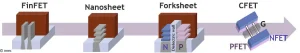
A roadmap for transistor architectures
“Today, the semiconductor industry is in a transition period from FinFET to Nanosheet, a device architecture that will extend the roadmap with multiple logic technology generations,” said Hans Mertens, principal member of technical staff at imec.
“Along the road, we might introduce the forksheet, an advanced nanosheet architecture that we proposed a few years ago, with reduced separation between adjacent devices, offering both scaling and performance advantages compared to conventional nanosheet,” he said.
“Towards the end of the decade, we expect the complementary FET (CFET) to enter the roadmap. In this device architecture, n- and pMOS devices are stacked on top of each other, removing for the first time the n-p separation from standard cell height considerations. When complemented with advanced technologies to contact the transistors, CFET will allow to gradually push track heights from 5T to 4T and even beyond, effectively shrinking standard cell size substantially.”
From processing point of view, CFET fabrication is challenging due to the nMOS-pMOS vertically stacked structure, and Mertens say imec is in the early stages of pathfinding. Several types of CFET have been proposed, with different construction techniques. In a sequential process flow, top-tier devices are processed sequentially after transfer of a blanket semiconductor layer by wafer bonding on top of bottom-tier devices. Monolithic integration involves building the vertical device architecture on a single substrate.
Monolithic CFET
imec is focussing on developing a monolithic CFET process as this offer the fastest path to CFET introduction for chip makers.
“Within our logic program, imec and its partners focus on monolithic CFET integration, as this integration scheme is the least disruptive compared to existing nanosheet-type process flows,” said Anne Vandooren, principal member of technical staff at imec.
“Nevertheless, the vertical stacking of layers from which both devices will be fabricated drives a need for high-aspect ratio patterning, selective deposition and removal of materials, and the deposition of high-quality (epi-)films. In addition, some CFET-specific process modules will need to be introduced to enable vertical isolation in the gate and contact part of the cross-section.
“We address these challenges by partitioning the monolithic CFET integration challenge into different sub-projects, with gradually increasing integration complexity. Each sub-project builds on a different test vehicle,” she said.
The first focus is on unipolar monolithic CFET, with n and p top and bottom devices processed on different wafers. The other test vehicles will have monolithic CMOS CFET devices processed on the same wafer.
These mainly differ in the way the CFET devices are contacted, eventually working towards advanced middle-of-line (MOL) and backside connectivity options. For each of the test vehicles, imec is exploring various process and integration options, trading off power-performance-area gains against complexity.
CFETs on a 48nm pitch
imec was the first to demonstrate monolithic CFET devices on a 300mm wafer in 2020, although at a ‘relaxed’ gate pitch (i.e., contacted poly pitch (CPP)) of 90nm. At VLSI 2023, imec presented unipolar CFET devices built through monolithic integration at industry-relevant 48nm gate pitch. The functional devices showed excellent switching characteristics for bottom and top devices separately, for both n- and pMOS and imec is currently exploring unipolar monolithic CFET integration at even smaller gate pitch.
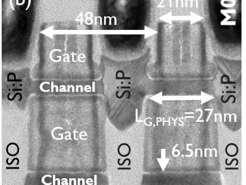
“In this demonstration, the source-drain epitaxial structures (source-drain epi) and source-drain contacts are evaluated for either bottom or top devices,” said Martens. “In addition, to limit the aspect ratio and be faster in the development, the active part of the structure was limited to only one nanosheet for the bottom and one for the top device. The significance of this work, however, is to show that, with a vertical separation of only 30nm between top and bottom sheets, we found a way to independently contact top and bottom devices. It is a steppingstone for advanced CFET integration at scaled dimensions.”
Stacked p-bottom and n-top devices will now be implemented on the same wafer and contacted independently. In addition, the integration flow should allow differentiating the threshold voltage (Vt) setting on the two devices that share a common gate, all at an industry relevant gate pitch of 50nm.
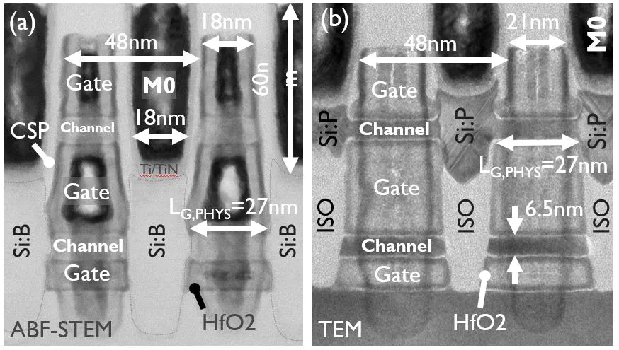
End-of-process cross sectional images for (a) bottom pFET and (b) top nFET (LG,PHYS=27nm) (as presented at VLSI 2023).
This vertical architecture has major implications. It requires not only the development of three new, CFET-specific process modules, but also adjustments to the other modules in the process flow to accommodate the presence of these CFET-specific modules.
“A first CFET-specific process module, which we refer to as the middle dielectric isolation (MDI), stems from the need to create a vertical dielectric isolation between top and bottom gate to differentiate on the Vt setting between top and bottom devices,” said Steven Demuynck, scientific director at imec.
“In addition, we continue our efforts to enable monolithic CMOS CFET device demonstration, a project strategic to imec, enabled by intense collaboration with our partners. To enable this, our team proposed a unique solution that affects the process flow from the start: the Si/SiGe stack, formed to create the active part of the CFET, is turned into a taller Si/SiGe1/SiGe2 multilayer stack, with higher Ge percentage for SiGe2 than for SiGe1.
“While sacrificial SiGe1 layers are replaced with the work function metals setting the Vt, the Ge-rich sacrificial layers are converted into the MDI dielectric creating the n-p WF metal separation within the gate. The stack allows for the formation of an inner spacer on the Ge-deficient layer in the stack – a critical nanosheet-specific feature that isolates the gate from the source-drain. Finding the most efficient way to co-integrate the bottom source-drain, the new MDI module and inner spacer at this tight pitch and for high aspect ratio geometries is currently the focus of our R&D effort.”
A second vertical isolation is needed between the source-drain contact metals of the top and bottom devices. Various options are explored to build and isolate bottom and top contacts – deep in between two tall gates – and subsequently route bottom and top transistors. A morphological proof of concept flow demonstrating the capability to fabricate a stacked MOL was shared at VLSI 2023.
“Finally, we need to encapsulate the top channel when growing the source-drain epi on the bottom device. This will effectively enable growing differentially doped epi on bottom and top devices,” he said.
Backside connection
“In the longer term, we are exploring advanced integration options to connect the active devices from the backside,” said Vandooren. “The developments are driven by the need to further reduce standard cell heights and avoid routing congestion in the back-end-of-line at the frontside of the wafer.
Backside contacting introduces additional process steps, including wafer bonding and substrate thinning from the backside. These steps challenge a very tight overlay for aligning the backside layers to the small features already present in the frontside. This is even more challenging as wafer deformation occurs during bonding, requiring the use of specific lithography overlay correction methods. In addition, an extra process module is needed to provide proper isolation between the backside metal 1 and the active nanosheet part of the CFET device.
“Since we started CFET development, we have been seeing an increase in the intensity of engagement with our equipment suppliers,” said Demuynck. “On the one hand, these vendors want to be involved in a very early stage of development to be able to identify where their tools, processes, and materials may fit into this roadmap. They also want to understand the context in which these would need to operate, to create awareness of interactions up- and downstream in the flow.”
imec plays a pivotal role in supplying these companies with wafers that have CFET-relevant topologies and geometries. Such material is usually not readily available to them before development begins at IDMs. On the other hand, these collaborations bring benefits for imec as well.
“The collaboration with our tool vendors helps us tap into the most advanced capabilities of our partners. In parallel, our logic core partners take an interest in identifying the key challenges and potential roadblocks that we encounter by evaluating various flow flavours. Understanding at an early stage what hardware and processes are enabling, can give them a head start in embarking on a R&D effort on their part,” he said.
 If you enjoyed this article, you will like the following ones: don't miss them by subscribing to :