Biodegradable PCB targets short-lifetime electronics
Researchers at the University of Glasgow have developed an almost entirely biodegradable PCB using zinc conductors and bio-derived substrate materials. The work aims to reduce the environmental impact of electronic waste by replacing conventional copper-based PCBs in applications designed for short operational lifetimes.
For eeNews Europe readers, the research is relevant as it explores alternative PCB materials and manufacturing methods that could be applied to disposable and low-duty-cycle electronics, including sensing and IoT-related devices.
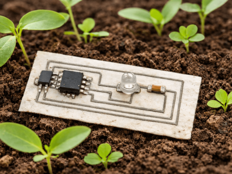
Additive manufacturing with zinc conductors
The approach differs from conventional PCB fabrication, which typically involves etching copper from a full sheet. Instead, the researchers use what they describe as a growth and transfer additive manufacturing process, depositing conductive material only where tracks are required. According to the team, this reduces metal usage and avoids the use of harsh chemical etchants.
Zinc is used as the conductive material rather than copper, despite having around one-third of copper’s conductivity. The researchers state that zinc remains sufficiently conductive for many applications, and that increased track thickness can be used to compensate for lower conductivity, with overall costs remaining comparable due to zinc’s lower material price.
The conductive tracks, reported to be as narrow as five microns, are transferred from a temporary carrier onto biodegradable substrates such as paper, bioplastics, and other bio-derived materials.
Performance, lifespan, and degradation
The team reports that the resulting circuits perform comparably to traditional boards and have been successfully tested in demonstrator devices including tactile sensors, LED counters, and temperature sensors. Performance stability was observed after more than one year under ambient storage conditions.
The work targets electronics intended for short lifetimes, such as disposable sensors, smart labels, and electronic pregnancy tests. The researchers estimate a shelf life of at least two years for devices produced using the process, although they note that further real-world testing is required.
In composting conditions, the circuits are expected to stop functioning within 24 hours, with full degradation occurring over several weeks. Protective coatings can be applied to delay degradation, but the researchers highlight a trade-off between environmental resistance during use and the ability to degrade at end of life. As a result, protection levels would need to be application-specific.
The team emphasises that fully biodegradable PCBs are not intended for long-lived, high-value electronics such as smartphones or computers, where extending operational lifetime and improving recyclability remains preferable.
Manufacturing challenges and environmental impact
Multilayer circuit fabrication remains a technical challenge, particularly the creation of through-hole interconnections between layers. Methods such as laser drilling are being investigated, although added complexity increases cost, meaning early demonstrator devices are likely to remain relatively simple.
A life cycle assessment comparing the biodegradable PCBs with conventional boards indicated a potential 79% reduction in global warming potential and a 90% reduction in resource depletion. The researchers also note that power sources remain a limiting factor, as conventional lithium batteries are not biodegradable, prompting parallel work on degradable battery technologies based on materials such as zinc, carbon, and gelatine.
The research was published in the journal Communications Materials and carried out at the University of Glasgow’s James Watt School of Engineering.
 If you enjoyed this article, you will like the following ones: don't miss them by subscribing to :