
AI optimisation for hybrid metrology in semiconductor process
SandBox Semiconductor in the US has developed an AI tool that works with data from different metrology tools to speed up the physic-based modelling of the chip-making process.
“When I set out to build SandBox the goal was to build something that engineers could use to accelerate their process development but what would be really cool is to do design technology co-optimisation across the value chain. That’s a long way off but we want to start to use it to inform the design rather than rely on rule based methods,” said Meghali Chopra, CEO and founder of Sandbox Semiconductor tells eeNews Europe.
The company emerged from Chopra’s research into plasma process optimisation and combines physic-based modelling with AI to speed up simulations and process recipe development.
“We use the simulations to predict the visualisation for all the possible process outcomes, such as minimising bowing in 3D etched structures so that you can do 15 experiments rather than 64 experiments.
- Lam Research pits process engineers against AI
- Merck teams for AI semiconductor process development
- Nvidia boss pitches generative AI for chip manufacturing
“One of the hardest things for the physics-based models is the 3D architectures so our database takes data from a variety of metrology including image processing to build a prediction of what the structure looks like and then figure out what the process optimisation should be. So we build visualisation tools with recipe development tools,” she said.
All of this uses data on the premises. “We are automating the machine learning pipeline on prem for the engineers to build the models themselves,” she said
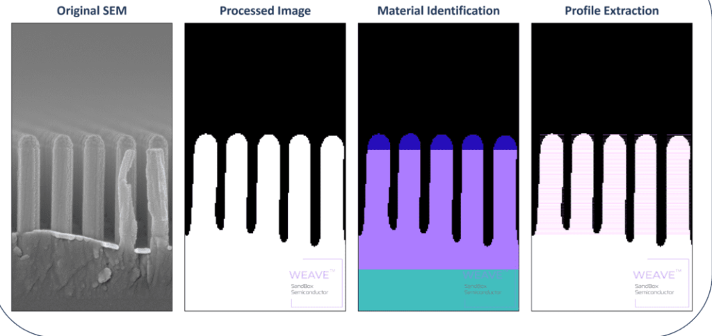
3D structure image analysis in Weave
The latest tool in the Sandbox Studio AI is Weave, which combines data from a range of metrology tools including scanning electron microscopy.
One of the biggest challenges in the semiconductor industry is developing manufacturing processes for increasingly advanced chip designs with high yield and reliability. Fabrication processes typically involve over a thousand steps that each must be carefully controlled and optimized. Today, this optimization is largely performed by iterative trial and error and requires companies to invest heavily in process development and recipe scaling to meet increasingly stringent manufacturing requirements. As chip technology advances with more 3D structures, the complexity of the fabrication process continues to increase.
The company works with foundries, memory chip makers and equipment makers. “Our customers are really struggling with the 3D structures and the metrology, and with our approach it’s easy to see where the metrology is inconsistent,” said Chopra
“We just released the Weave with automated cross section SEM and TEM images to output a segmented image, extracting the feature profile and output to confirm that it met the recipe targets,” she said. “We take in empirical data cross sectional information and cross wafer data and build a model that gives a recipe scorecard. It takes about three days to build model to output the simulated model outcome.”
“Hybrid metrology approaches that combine data gathered from multiple toolsets are becoming increasingly necessary, particularly in the era of 3D NAND, DRAM, and gate-all-around architectures, to address the complexity and spectrum of measuring tasks involved in developing a leading-edge process. With our new metrology automation features, engineers can now use our platform to manage and analyze multi-modal data to gain process insights, predict outcomes, and ultimately develop new processes not possible before,” said Chopra.
 If you enjoyed this article, you will like the following ones: don't miss them by subscribing to :