AI chiplet tech creates 100 x 100mm packages
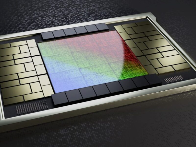
Sarcina Technology has developed a AI chiplet platform that can create systems as large as 100 x 100mm in a single package.
The platform uses the FOCoS-CL (Fan-Out Chip-on-Substrate-Chip Last) assembly technology from packaging giant ASE, adding an interposer which supports chiplet designs using the UCIe-A standard.
This die-to-die interposer enables AI customers to use chiplets to form large silicon areas, supporting high-performance computing with higher wafer yields than monoliothic devices and combining different technologies.
This large package design allows for the integration of more memory, which is crucial for generative AI applications that require rapid, parallel data processing.
The Sarcina team has successfully developed an interposer with up to 64 bits of data interface per module, achieving data rates of up to 32 GT/s. This delivers the highest UCIe-A performance in terms of both bandwidth and data rate, as specified by the UCIe 2.0 standard.
The key point is that FOCoS-CL is a more cost-effective replacement for costly 2.5D TSV (Through-Silicon Via) silicon interposer technology or silicon bridge die with fan-out RDL interconnections.
Multiple modules can be arranged in parallel along the silicon die edge and there is also a choice between up to 20 LPDDR5X/6 packaged memory chips or eight and HBM3e memory stacks. LPDDR6 memory also incorporates 3D stacking technology similar to HBM, achieving data rates of approximately 10 GT/s.
All this allows the creation of chip measuring 100 x 100mm with power consumption up to 500W with forced air cooling and up to 1000W with liquid cooling, offering flexible deployment options in the datacentre.
“Six years ago, after prototyping a 2.5D silicon TSV interposer package that integrated one ASIC and two HBMs, we predicted this technology would enable highly complex compute solutions. Today, this vision is becoming a reality, driven by RDL die-to-die interconnects like UCIe,” said Dr. Larry Zu, CEO of Sarcina Technology:
“With FOCoS assembly technology, we are entering a new era of AI computing. Our AI platform offers greater efficiency and customization, with the lowest cost in the industry for generative AI chips. This ensures that our customers stay competitive in the rapidly evolving AI landscape.”
The chiplet packaging platform allows semiconductor startups to focus on developing efficient algorithms for generative AI and edge AI training without the need for an expensive post-silicon design and manufacturing team, says Zu. Startups can develop their silicon and pass it to Sarcina for post-silicon packaging, streamlining the process and reducing costs while maintaining high performance.
 If you enjoyed this article, you will like the following ones: don't miss them by subscribing to :